
THE CALIFORNIA DEFENSE READY ELECTRONICS AND MICRODEVICES SUPERHUB
Integrating SWAP and MMEC Technologies into MOSIS 2.0
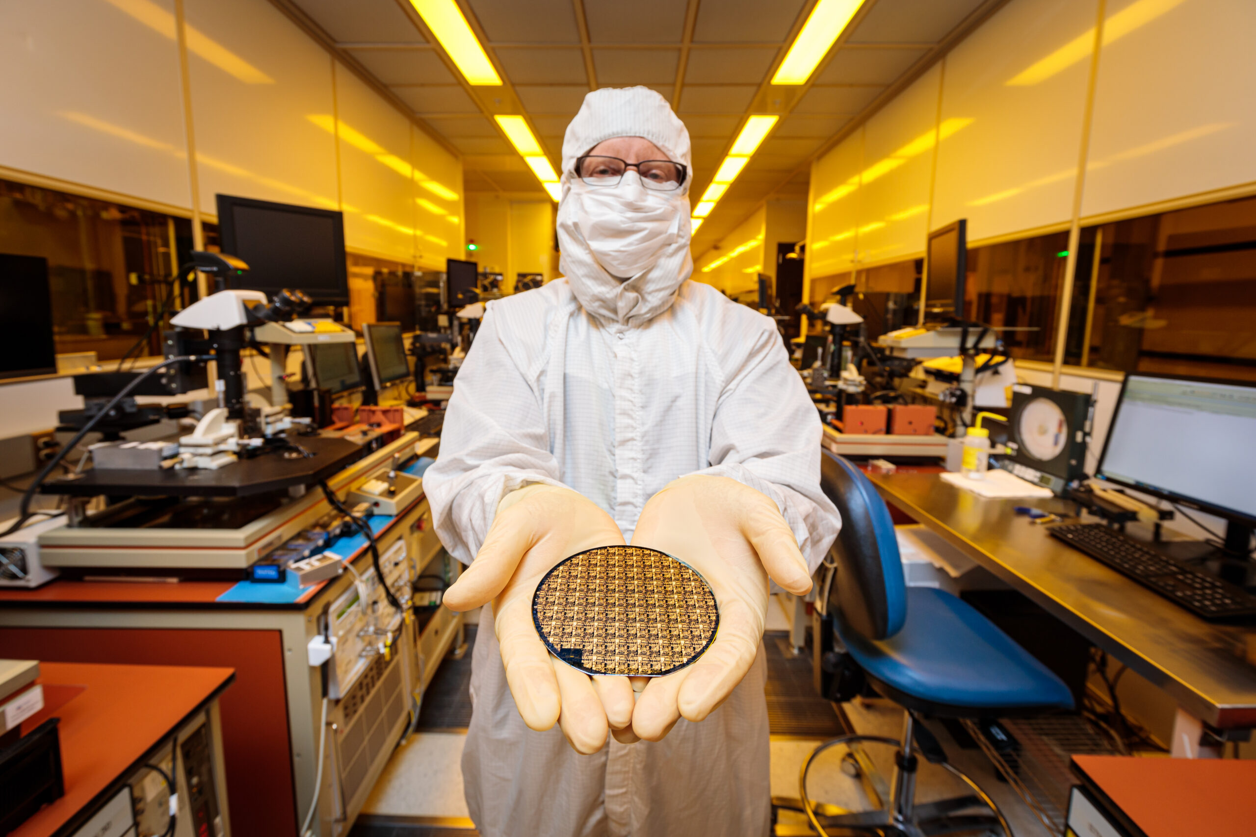
In 2025, MOSIS 2.0, is significantly expanding its semiconductor prototyping capabilities beyond Southern California to include technologies from two additional technology hubs: the Southwest Advanced Prototyping (SWAP) Hub, led by the Arizona Board of Regents on behalf of Arizona State University, and the Midwest Microelectronics Consortium (MMEC) Hub in Ohio.