ISI News
California DREAMS Showcases Semiconductor Impact on the National Stage
The California Defense Ready Electronics and Microdevices Superhub (CA DREAMS), led by the University of Southern California Information Sciences Institute (USC ISI), took a national spotlight at the 2026 Microelectronics Commons Annual Meeting, showcasing two years of growing impact and leadership in domestic semiconductor prototyping.
Held from February 18–20 at the JW Marriott in Washington D.C., the summit convened leaders from the U.S. Department of War, industry and academia to assess progress across the eight regional hubs of the Microelectronics Commons.
Opening the event, Hon. Mike Dodd, Assistant Secretary of War for Critical Technologies and acting Deputy Director of the Defense Innovation Unit, underscored the strategic importance of the hub model.
“The mission of the Commons is clear and direct,” Dodd said. “Our goal revolves around the creation of a robust network of hubs to accelerate domestic prototyping, secure the supply chain, and bridge that gap from lab to fab that separates laboratory breakthroughs from commercially viable fabrication.”
Dodd highlighted the impact of the hubs, noting the successes of CA DREAMS.
“The California DREAMS Hub, based out of the University of Southern California, has cut in half the time to develop and fabricate state-of-the-art RF chips and phased arrays for 5G, 6G, and electromagnetic warfare applications,” he said. “They have demonstrated transition of these technologies from their university labs to U.S.-based fabrication at industry powerhouses like Northrop [Grumman], HRL, and Teledyne.”
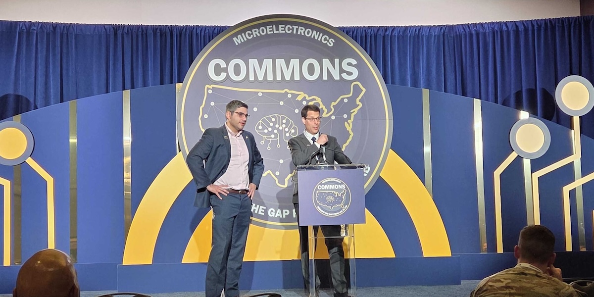
CA DREAMS Director Steve Crago said that the ME Commons annual meeting was a critical event for the microelectronics sector in the United States, providing the invaluable opportunity for the CA DREAMS team to connect with Commons leadership, government, congressional staffers and colleagues across the hubs.
Crago, who is also Associate Director of USC ISI, presented the CA DREAMS hub overview, along with Andrea Belz, USC Viterbi Vice Dean of Transformative Initiatives, and Rehan Kapadia, Director of MOSIS 2.0, the semiconductor fabrication service at the heart of CA DREAMS. The overview highlighted the impact of MOSIS 2.0, the latest CA DREAMS initiatives to build the semiconductor workforce talent pipeline, and the success of key projects for 5G, 6G and electronic warfare.
“Our goal is to make sustainable, accelerated prototyping the norm, not the exception,” Crago said. “MOSIS 2.0 is connecting a growing number of developers with research and fabrication, to bridge that critical gap between innovation and realization. We are rapidly expanding our network of foundries and service providers, and we have launched new partnerships with our ME Commons hub colleagues at Midwest Microelectronics Consortium (MMEC) and Southwest Advanced Prototyping Hub (SWAP).”
“The time savings we’ve already demonstrated in the lab-to-fab pipeline shows that when you connect advanced compound semiconductors, silicon platforms and packaging under MOSIS 2.0, you can fundamentally change the speed of innovation,” Crago said.
MOSIS 2.0: a Semiconductor Prototyping Powerhouse
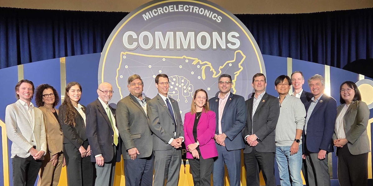
The CA DREAMS and MOSIS 2.0 delegation at the Microelectronics Commons Annual Meeting.
A central focus of the CA DREAMS overview was MOSIS 2.0, which Kapadia described as an engineering-driven gateway connecting academic, defense and commercial customers to high-volume foundries, defense industrial base fabs and seven university nanofabrication facilities.
“We have expertise in circuit design, packaging and fabrication,” Kapadia said. “With that engineering team, we are able to work with academic customers, DoW customers and commercial customers, and then give them access to a wide variety of capabilities.”
Those capabilities span leading-edge commercial nodes — including GlobalFoundries, Intel, Samsung and TSMC — as well as mid-volume and compound semiconductor partners such as Northrop Grumman, Teledyne and HRL.
Kapadia, the Colleen and Roberto Padovani Early Career Chair in Electrical and Computer Engineering at USC, noted the rapid growth of customer engagement with MOSIS 2.0.
“We have probably about 200 to 300 customers that we’ve engaged with, and we expect probably about 50 to 100 tape-outs to run through us this year,” he said.
Beyond traditional multi-project wafer (MPW) services, MOSIS 2.0 is introducing new acceleration tools, including IP repositories, AI-driven circuit design support and MOSIS Advanced Prototyping Platforms — semi-customizable field programmable gate array (FPGA)-based systems that shrink the time from initial design to tested hardware.
Kapadia also detailed a major expansion in fab analytics across the hub’s seven nanofabs. Through real-time data collection and process modeling, CA DREAMS has demonstrated one-shot process transfers between facilities — reducing what historically required 10 experimental runs to a single transfer.
The result: a faster, lower-risk pathway from lab innovation to scalable fabrication.
Two Years of Rapid Momentum: AmmP3 and GaNAmp
With MOSIS 2.0 as its backbone, CA DREAMS highlighted two flagship technical efforts led by hub partner and leading global and aerospace defense technology company Northrop Grumman: the Accelerated Millimeter Wave Phased Array Prototype (AmmP3) project and the GAN Amplifier Prototypes project (GaNAmp).
Monte Watanabe, Manager of Electronics Engineering at Northrop Grumman’s Microelectronics Center, and AmmP3 project lead, said that communications was of utmost importance to warfighters in harm’s way, which is why advancing millimeter-wave phased arrays for defense applications was so critical.
With $28.3 million in funding from the DoW, the AmmP3 project focuses on electronically scanned arrays using 3D heterogeneous integration to combine high-performance III-V microelectronics with commercial silicon platforms. AmmP3 has reduced phased-array prototyping time by a factor of two while targeting a 10-fold improvement in range and bandwidth.
“Typically, these cycles to develop these highly integrated arrays take very long — two to three years in my experience,” Watanabe said. “What we’re trying to do is improve that speed so we can get those prototypes out there, get them in the hands of the folks that are making decisions and requirements for the warfighter.”
Alex Zamora, RF and Mixed-Signal Department Manager at Northrop Grumman’s Microelectronics Center, presented year-one results from GaNAmp, a $33.7 million DoW-funded effort advancing gallium nitride (GaN) technologies for electronic warfare. GaN is a next-generation semiconductor material with a wide bandgap, offering superior efficiency, faster switching, higher temperature tolerance, and smaller form factors compared to traditional silicon.
“The goal of our project is to enable higher power, higher efficiency, and spectrum-dominant solutions for electronic warfare objective systems,” Zamora said.
He emphasized that success required advancement across the full technology stack.
“You have to make advancements at the material, the device, the integrated circuit, and the fully packaged subsystem level,” he said. “On this project, we’re making advancements at every single level of technological hierarchy.”
Zamora highlighted the sustainability of the hub model.
“From the inception of our project, we had the California DREAMS Hub sustainability model in mind,” he said, describing how material maturation, accelerated IC prototyping and system-level packaging generate a permanent storefront capability through MOSIS 2.0.
Fostering Future Microelectronics Industry Leaders
In addition to showcasing technological offerings and partnership growth, CA DREAMS highlighted its unique data-driven strategy to attract and grow a talent base that will meet the critical future workforce needs of the semiconductor industry.
Belz, who leads the DREAMS Workforce Development program, noted that Southern California represents roughly 5% of the national semiconductor workforce, with about 1,100 unique employers.
To better understand regional needs, CA DREAMS recently launched JobPulse, an intelligence platform analyzing real-time job postings to estimate labor market demand.
“Most notable is the fact that we estimate that the ratio of engineers to technicians needed is about 3 to 1, which differs strongly from the published numbers of 1 to 2,” Belz said. “In terms of the need for scientists, the demand for PhD-level scientists outstrips PhD production numbers by orders of magnitude. We just can’t produce enough PhDs to meet the need.”
In response to these urgent issues, CA DREAMS has launched a hands-on training program, the Cleanroom Gateway, which introduces participants to the environment, tools, and practices of semiconductor microfabrication, preparing them for further training or employment in the field. This program is backed up by a national train-the-trainer model to scale cleanroom education across all hubs. The hub partners with IEEE to offer industry-recognized microcredentials for students in the operation of specialized laboratory equipment and cleanroom safety protocols. Belz outlined how math engagement and Discovery Days at the USC John O’Brien Nanofabrication Laboratory feed into the STEM education pipeline for K-12 students.
A National Model for Lab-to-Fab Transition
Crago said that the Microelectronics Commons meeting was a vital platform for CA DREAMS to demonstrate how the USC-led hub is accelerating lab-to-fab transition at scale, a critical model for the future growth of semiconductor technology in the United States.
“By combining MOSIS 2.0’s national storefront, our hub partner breakthroughs and our data-driven workforce development initiatives, the USC-led hub at CA DREAMS is advancing a coordinated, domestic ecosystem for next-generation microelectronics,” Crago said.
Distribution Statement A: Approved for public release. Distribution is unlimited.