ISI News
CA DREAMS and Northrop Grumman Push Semiconductor Projects into High Gear

When the California Defense Ready Electronics and Microdevices Superhub (CA DREAMS) and Northrop Grumman launched two landmark semiconductor projects, the ambition was clear and bold: prove that American industry could develop cutting-edge defense electronics in a fraction of the time it traditionally takes. A year later, the initial results are in, and the teams are already raising the bar.
The two projects — GaNAmp, which focuses on gallium nitride power amplifier technology for electronic warfare, and AmmP3, which is building a prototype and toolkit for next-generation millimeter wave communications systems — have each delivered promising early milestones. Now, in year two, the mission shifts from proof-of-concept to real-world impact: faster cycles, harder performance targets, and prototypes ready to move out of the lab and into the field.
Together, the projects represent $30M in investment in project year 2, after an initial investment of $32M in the first year under the Department of War’s Microelectronics Commons Program. CA DREAMS is led by the USC Viterbi School of Engineering’s Information Sciences Institute (ISI), with Northrop Grumman leading technical execution on the two projects.
Amplifying the Signal: GaNAmp Targets World-Class Performance
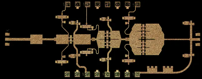
Intricate circuitry of Northrop Grumman’s high-frequency Gallium Nitride chip that operates at W-band, the highest output power of a commercially available chip. Image/Northrop Grumman
Gallium nitride (GaN) is a remarkable semiconductor material. Unlike the silicon chips found in everyday consumer electronics, it can withstand extreme heat and power levels, making it ideal for the high-power amplifiers used in electronic warfare (EW) systems. However, turning GaN laboratory breakthroughs into production-ready hardware has historically been painfully slow.
That is exactly what CA DREAMS and Northrop Grumman’s GaNAmp project sets out to change. The project draws on university research, advancing GaN manufacturing capabilities across four key domestic foundries (Northrop Grumman, HRL, Teledyne, and Monde/Transphorm), and developing smarter ways to assemble and package finished chips. Together, these efforts aim to continue delivering shorter development timelines and high-performance amplifier solutions ready for real-world applications.
Alex Zamora, the project lead and RF/mixed-signal department manager at Northrop Grumman, said the project spans the full chain, from raw material to deployable system.
“It aims to advance gallium nitride material systems at the foundation. But not only are we advancing the materials, we are synthesizing devices that leverage the materials, and then we are taking those devices and making integrated circuits to get functionality out of the transistor technology,” Zamora said. “Then we are taking it a step further, where we take those integrated circuits and synthesize actual subsystems for electromagnetic warfare applications.”
For those subsystems, the practical payoff is significant. A more powerful GaN amplifier means an EW system can transmit signals further, improving military capability.

Alex Zamora. Image/Northrop Grumman
In year one, the team delivered. GaNAmp produced repositories of world-class chips that operate across a wide frequency range and demonstrated subsystem-level performance using those gallium nitride components. Critically, the team also slashed prototyping timelines. Chip fabrication runs that would typically take six to eight months were completed in under four.
Part of that acceleration came from a partnership with high-performance radio frequency (RF) chip manufacturer, PseudolithIC, which found a way to decouple advances in chip design from advances in the underlying transistor technology, allowing both to progress simultaneously rather than sequentially.
Year two sets a considerably higher bar. Requirements are what Zamora calls state-of-the-art — meaning the team is not just trying to improve on its own previous results, but produce the best performance metrics of any GaN program in the world.
“If we’re not doing best in the world, then we’re just another gallium nitride program,” Zamora said.
The year two project goal is to move GanAmp beyond the lab to produce prototypes that can be used directly in the field.
Building the Toolkit: AmmP3 Accelerates Millimeter Wave Adoption

Monte Watanabe. Image/Northrop Grumman
The second project, AmmP3, is tackling a different but equally important challenge: making it dramatically easier and faster to design and build systems that operate at millimeter wave frequencies.
Millimeter waves occupy a higher frequency band than conventional cell phone signals, which means they can carry far more data, and are harder to intercept. That makes them attractive both for next-generation 5G and 6G commercial networks and for defense communications and sensing applications. The difficulty is physics: at higher frequencies, signals lose energy more quickly over distance.
Monte Watanabe, RF/mixed-signal assistant department manager at Northrop Grumman and the AmmP3 project lead, explains how phased arrays solve that problem.
“The phased array allows us to efficiently focus the energy in the direction that we want, versus radiating it all over the place. By focusing the energy, we’re able to reduce the amount of power that we need to transmit, and it enables systems that are lower power to be able to operate at higher frequency,” Watanabe said. “Think of your cell phone. You don’t have to worry about which way it’s pointing. It connects because it’s radiating in all directions. But at higher frequencies, we need an advanced way of sending the information in the right direction. The phased array is what allows us to do that.”
For defense users, the appeal goes beyond bandwidth. Higher-frequency signals are not only more data-rich — they’re also more secure.
“Because it is harder to transmit that information, it’s also harder to receive, so it’s more protected,” Watanabe said. “Wider bandwidth, more data, you can do more things with it, and it is harder to access. That’s the uniqueness of why we want to move to higher frequencies.”
Building these systems has historically required years of specialized development, in large part because the expertise and components needed are scattered across several organizations. The AmmP3 project’s solution will be a unified, accessible toolkit — drawing on contributions from Northrop Grumman, Teledyne, UCSB, UCSD, and other hub partners — that gives engineers a ready-made starting point rather than forcing every team to begin from scratch.
That toolkit will be made available through CA DREAMS’ MOSIS 2.0 prototyping storefront — a one-stop service where engineers and organizations can access hub capabilities for their own millimeter wave development needs.
In year one, the team made real progress on the timeline challenge. Traditional phased array development cycles run to about 36 months. The AmmP3 project landed on an 18-month cycle.
Year two builds on that momentum with higher ambition. Northrop Grumman is incorporating advanced GaN technology into its AmmP3 work, targeting a tenfold improvement in prototype performance relative to year one. For the first time, the project also introduces radiation-hardened digital integrated circuits — a technology with implications that go well beyond communications, making electronics viable in space and other extreme environments.
Building a New Model for American Innovation

Steve Crago, CA DREAMS director and associate director of ISI.
The two projects represent something larger than their individual technical achievements. Both Zamora and Watanabe point to the collaborative model itself — industry, universities, and government working in close coordination — as the real innovation on display. For Steve Crago, CA DREAMS director and associate director of ISI, year one validated the fundamental bet that the hub model could work.
“Year one demonstrated that this model of concentrated, collaborative effort genuinely works,” Crago said. “Northrop Grumman and our university and industry partners didn’t just deliver prototypes — they proved that the whole is greater than the sum of its parts. Seeing world-class chips and subsystems come out of this team in less than twelve months is exactly the kind of result that makes us confident in what we’re building together.”
For Watanabe, the most meaningful outcome of year one was not any single prototype, but the proof that the team could function as a cohesive unit.
“Overall, for CA DREAMS and Microelectronics Commons, the ability to bring these diverse teams together and demonstrate real capability — and then looking forward to year two, where we’re taking that and expanding upon it and improving it, using that same team, that same recipe — just shows what CA DREAMS brings to bear, and what ME Commons is doing for the microelectronics industry in America.”
With year two now underway and both projects targeting demonstrations that were unimaginable under traditional development timelines, the CA DREAMS model is beginning to deliver on its central promise: that when the full power of Southern California’s research and industry ecosystem is focused on a single challenge, the pace of innovation can be transformed.
Crago sees year two as a chance to build on that foundation and deepen the hub’s impact on U.S. defense readiness.
“Year one showed us what this team is capable of,” Crago said. “Now, in year two, we can take those breakthroughs and push them toward real deployment. That is exactly why CA DREAMS was created, and exactly what the Microelectronics Commons program was designed to achieve.”
Distribution Statement A: Approved for public release. Distribution is unlimited.