ISI News
MOSIS 2.0 and GlobalFoundries Partnership: A Strategic Alliance for Semiconductor Innovation
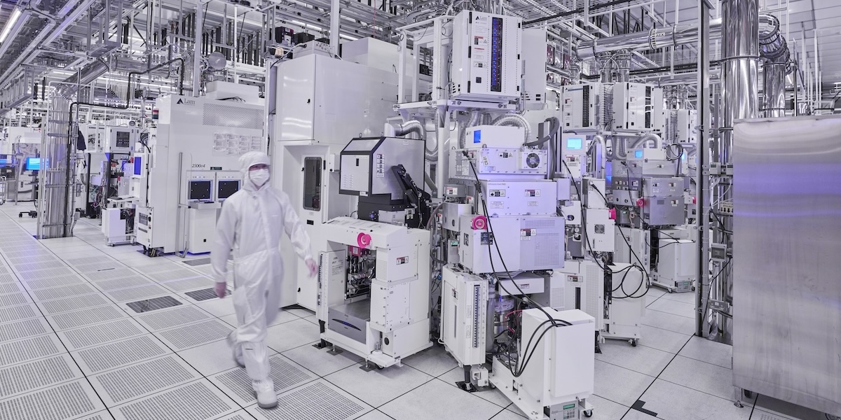
MOSIS 2.0 and GlobalFoundries have formed a strategic value-added partnership that enables customers to access GF technologies, including cutting-edge FinFET and FDX™ FD-SOI process technologies, through MOSIS 2.0’s storefront platform, creating a pathway for rapid and cost-effective prototype development via shared shuttle runs to full-scale commercial production with dedicated mask sets.
By eliminating traditional barriers between research and manufacturing, this collaboration democratizes access to sophisticated semiconductor capabilities while strengthening domestic supply chains and reducing dependence on overseas fabrication for American innovators, startups, and established companies alike. The GlobalFoundries agreement is now active, with MOSIS 2.0 actively onboarding users interested in both prototyping and production runs.
Breaking Down Barriers: Advanced Technologies Made Accessible
The collaboration addresses a fundamental challenge in the semiconductor industry: the gap between innovation and production-scale manufacturing.
“Thanks to this agreement, MOSIS 2.0 can now offer the full suite of GF technologies from U.S.-based fabs,” said Rehan Kapadia, Director of MOSIS 2.0, “a capability that significantly expands the technological horizon for researchers, startups, and commercial developers.”
“GlobalFoundries and MOSIS 2.0 are moving the industry forward, expanding access to GF’s differentiated technologies and advanced manufacturing capabilities to the innovators creating the next generation of essential technologies,” said Samuel Vicari, Chief Customer Officer at GF. “Through this new strategic partnership, we are adding important value to MOSIS 2.0’s extensive network of universities, research institutions and emerging technology companies as a manufacturing partner with the end-to-end services, support and U.S.-based manufacturing to unlock the full potential of their designs.”
For customers ready to scale their innovations, the partnership extends to full-mask production, where entire manufacturing runs are dedicated to single chip designs, eliminating the traditional barriers and complexities associated with moving from prototype to production.
This access spans the entire development lifecycle, from early-stage prototyping through commercial production: users can start with shared shuttle runs, where multiple designs are combined onto a single wafer to keep costs low during development, creating unprecedented continuity for chip designers. A comprehensive approach that allows designers to minimize costs during the critical development phase.
This cost-effective approach has long been MOSIS 2.0’s strength, making advanced semiconductor prototyping accessible to universities, startups, and small companies that couldn’t otherwise afford full-scale fabrication runs.
Simplifying Complex Relationships
One of the partnership’s most significant advantages lies in its simplification of the traditionally complex foundry-customer relationship. The MOSIS 2.0 team handles coordination and technical support throughout the entire process, helping users meet manufacturing requirements and navigate production timelines. This approach dramatically reduces the technical and administrative burden on customers, particularly smaller organizations that lack dedicated foundry liaison capabilities.
“This will really reduce the barrier for commercial users to use domestic manufacturing,” Kapadia noted, highlighting how the partnership addresses a critical need in strengthening U.S. semiconductor independence.
For MOSIS 2.0, this partnership represents a strategic evolution from primarily serving academic and research communities to becoming a comprehensive commercial semiconductor service provider. Access to GF’s FinFET and FDX platforms positions MOSIS 2.0 at the forefront of advanced semiconductor technologies. In addition to advanced CMOS, the platform also provides access to U.S.-based offerings in RF and silicon photonics—enabling development of sophisticated applications in AI, 5G/6G communications, automotive electronics, data centers, and other high-growth sectors.
National Security and Economic Implications
The partnership carries significant implications beyond commercial benefits, supporting broader U.S. strategic objectives in semiconductor independence and innovation leadership. MOSIS 2.0 is operated by CA DREAMS, one of the Microelectronics Commons hubs, operated by the University of Southern California (USC). By making advanced U.S.-based manufacturing more accessible, the collaboration helps reduce dependence on overseas fabrication while strengthening domestic semiconductor capabilities. By lowering barriers to advanced U.S. manufacturing, the partnership helps ensure that American innovations can be developed and produced domestically.
A Comprehensive Ecosystem Approach
MOSIS 2.0 continues to support the full spectrum of design needs by offering comprehensive semiconductor prototyping through a broad partner network and providing end-to-end support from design to testing. The goal extends beyond simple manufacturing access to encompass the entire chip development lifecycle, from academic research through commercial product launches.
Looking Forward: A New Model for Industry Growth
The MOSIS 2.0-GlobalFoundries partnership represents a new paradigm for semiconductor industry collaboration, one that recognizes the value of specialization while creating integrated pathways for innovation success. As the semiconductor industry continues evolving toward more specialized applications and greater emphasis on supply chain security, such partnerships become increasingly critical for maintaining competitiveness and driving innovation.
About MOSIS 2.0
MOSIS 2.0 is a national access platform for semiconductor design and manufacturing operated by CA DREAMS, one of the eight Microelectronics Commons hubs, at the Information Sciences Institute (ISI), part of the USC Viterbi School of Engineering. Building on the legacy of the original MOSIS service, which has supported more than 60,000 chip designs since 1981, MOSIS 2.0 connects users to U.S.-based foundries and advanced backend services. The platform enables researchers, startups, and commercial teams to move from prototype to production through a single point of access. It is designed to lower barriers, accelerate development, and expand domestic innovation. For more information, www.mosis2.com.
Contact: Greta Harrison, CA DREAMS Senior Content Developer, [email protected]
About GlobalFoundries
GlobalFoundries (GF) is a leading manufacturer of essential semiconductors, enabling AI at scale from the cloud to the physical world. Through deep partnerships with customers, GF delivers differentiated, power efficient and high performance solutions for automotive, aerospace and defense, data center, smart mobile devices, internet of things and other high growth markets. With global manufacturing operations across the U.S., Europe and Asia, GF is a trusted and holistic technology partner for customers around the world. GF’s talented, global team remains focused every day on security, longevity and sustainability. For more information, visit www.gf.com.
Contact: Stephanie Gonzalez, [email protected]
Distribution Statement A: Approved for public release. Distribution is unlimited.